
How are Xilinx 7 series FPGA pins defined?
How to download the FPGA pin file ( Pi noout file) during schematic design
1. Xilinx7 series FPGA pin definition
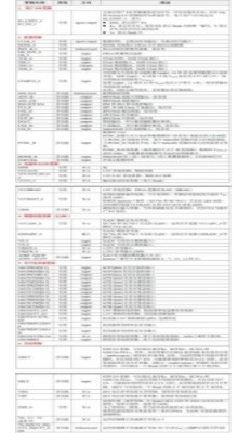
Table 1-1, Xilinx 7 series FPGA pin definitions
The device pins of the FPGA are divided into banks, and each bank is powered independently, so that the FPGA I/O can adapt to different voltage standards and enhance the flexibility of I/O design. Each user bank includes 50 I/O pins or 24 pairs of differential pair pins (48 differential signals), and a single-ended pin for Top and Bottom. Figure 1 shows an example of the K325T chip user Bank IO schematic diagram.
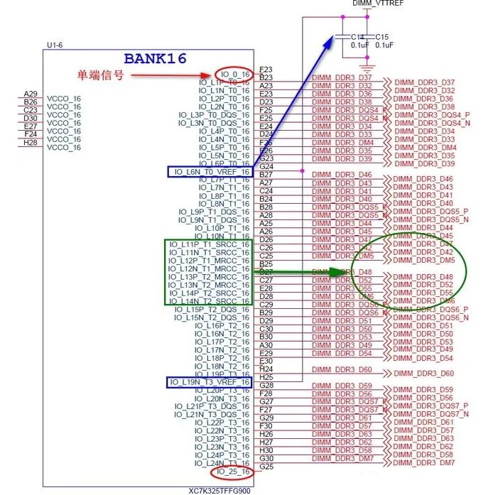
Figure 1. Schematic diagram of K325T chip user Bank IO
In the figure, we can see the two single-ended signals circled in red, the _CC clock pin circled by the green line can be used as user I/O when it is not used as a clock input, in addition, we can also see the blue The marked VREF pin, when the BANK I/O is used as a DDR memory interface , needs to provide the threshold voltage required by the pseudo-differential, and the _VREF_ pin needs to be connected to the reference voltage required by the DDR peripheral. For other I/O pin analysis, please refer to Table 1-1 pin definition description.
2. Xilinx7 series FPGA pinout file download
When we are designing the schematic library, how do we get the definition of each pin of the FPGA? In the ASCII Pinout Files subsection of the 7 Series FPGAs Package Files in Chapter 2 of the UG475 official document, according to the FPGA device family and device package classification, the pinout definition link addresses of all devices in the 7 series are given. The official website gives Pinout files in CSV and TXT formats, we can choose flexibly.
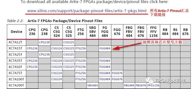
Figure 2. FPGA Pinout download link
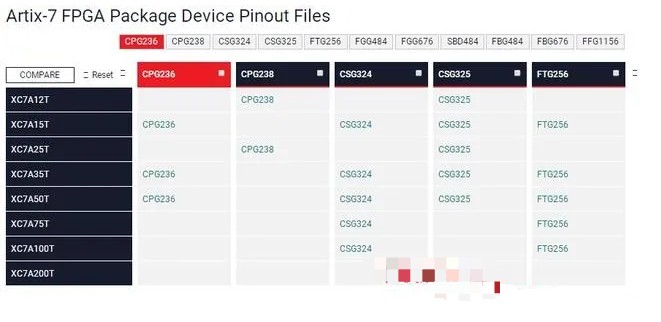
Figure 3. Download Pinout from Xilinx official website
We open a Pinout in the form of .TXT, as shown in Figure 4. It can be seen that the file is divided into 8 columns and contains all the key information required for the design schematic: pin number, pin name, pin DDR memory group, pin BANK number, auxiliary group (VCCAUX), super logic domain ( SLR), I/O pin type (configuration, HR, HP, transceiver pins, etc.), and NC pin information related to device Pin-to-Pin compatibility.
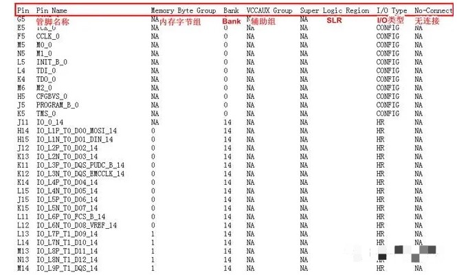
Figure 4. Example of Pinout file content
Detailed explanation of power supply design of Xilinx FPGA
Document This article mainly introduces the power supply design of Xilinx
xilinx fpga development software
Today let's talk about the XADC function in FPGA. XADC is a collection of ADC modules, temp
Mfmic introduces about what is the FPGA chips
The core idea of FPGA: 1. FPGA is a branch of digital chips. Unlike functional fixed chips such as
How are Xilinx 7 series FPGA pins defined?
How to download the FPGA pin file ( Pi noout file) during schematic design 1. X
CMOS image sensors used in cars are in short supply in 2022ï¼
According to MFMIC reported on May 12“In the automotive industry, as many chip suppliers focu
Online Marketplace for Electronic Parts
Start search parts now

2019
IC FPGA 360 I/O 665FCBGA
2019
IC FPGA 607 I/O 1020FBGA
IC FPGA 556 I/O 896FCBGA
IC FPGA 564 I/O 1152FBGA
IC FPGA 680 I/O 1738FCBGA
IC FPGA 320 I/O 668FCBGA
IC FPGA 768 I/O 1148FCBGA
IC FPGA 400 I/O 1156FCBGA
IC FPGA 440 I/O 676FCBGA
IC FPGA 488 I/O 780HBGA