
Block RAM in xilinx 7 series FPGA
A slice and a global clock together can implement any combinational logic and sequential logic functions, but in many cases we also need to temporarily store the data inside the FPGA for other purposes. As the most basic unit of FPGA, Slice can also complete the function of data storage, but it is obviously overkill. Therefore, xilinx has specially integrated many memory modules in its FPGA, called Block RAM, which is like a pearl in the sea of ​​slices. , specifically to realize the data temporary storage function, and each clock area is arranged with several Block RAMs.
Today we will talk about the Block RAM in the 7 series FPGA.
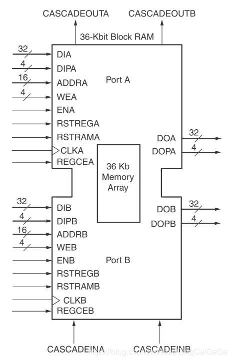
In the 7 series FPGA, each block RAM can store up to 36Kb of data, 2 block RAMs can be cascaded to achieve 64kb data storage, and each block RAM can be divided into 2 18kb block RAMs, nothing more, no more points, nor can they be cascaded infinitely.
When block RAM is used, it uses Xilinx CORE Generator for brainless configuration, which can be configured into RAM, ROM and the most widely used FIFO. RAM can be configured into various interface modes and readout modes, and FIFO can be configured as synchronous FIFO and asynchronous FIFO. All configuration information is implemented in the FPGA development tool Xilinx CORE Generator.
The various configurations of Block RAM and how to read/write data RAM and FIFO under the global clock are too many to describe, but they are very easy to use. Basically, you only need to get the following a few signals: clock, reset , clock enable, read data, read address, read enable, write data, write address, write enable, data empty signal, data full signal, later we will take it out separately and use a specific example to operate a wave!
Mfmic released the analysis report on the innovation index of electronic components in the first quarter of 2022
On May 16, 2022, MFMIC and the Organizing Committee of China Electronics Fair (CEF) officially relea
xilinx fpga development software
Today let's talk about the XADC function in FPGA. XADC is a collection of ADC modules, temp
Introduction to Xilinx 7 Series Four Types of FPGAs
The Xilinx 7 series FPGAs consist of four FPGA families addressing complete system require
MFMIC reports: Two EDA companies have won the favor of capital, with investors including CITIC 5G Fund and Huada Jiutian
Recently, CITIC 5G Fund completed the investment in XILINX EDA Enterprise Xinhuazhang. This round of
Mfmic introduces about what is the FPGA chips
The core idea of FPGA: 1. FPGA is a branch of digital chips. Unlike functional fixed chips such as
Online Marketplace for Electronic Parts
Start search parts now

2019
IC FPGA 360 I/O 665FCBGA
2019
IC FPGA 607 I/O 1020FBGA
IC FPGA 556 I/O 896FCBGA
IC FPGA 564 I/O 1152FBGA
IC FPGA 680 I/O 1738FCBGA
IC FPGA 320 I/O 668FCBGA
IC FPGA 768 I/O 1148FCBGA
IC FPGA 400 I/O 1156FCBGA
IC FPGA 440 I/O 676FCBGA
IC FPGA 488 I/O 780HBGA